Maverick Hoziel
Status as of January 30, 2026
The project followed a structured experimental workflow beginning with Mach–Zehnder modulator characterization, then extending to evaluation of the TFLN modulation platform, and culminating in link level assessment of IM/DD performance and signal integrity.
Phase 1 — Modulator Characterization
First, let us understand how a Mach–Zehnder modulator (MZM) operates. An MZM works by splitting an incoming optical signal into two interferometer arms. A relative phase shift is then introduced between the two paths. This phase shift can either be applied entirely to one arm as φ, or symmetrically as ±φ/2 across both arms. A visual illustration of the Mach–Zehnder interferometer used in this setup is shown below.
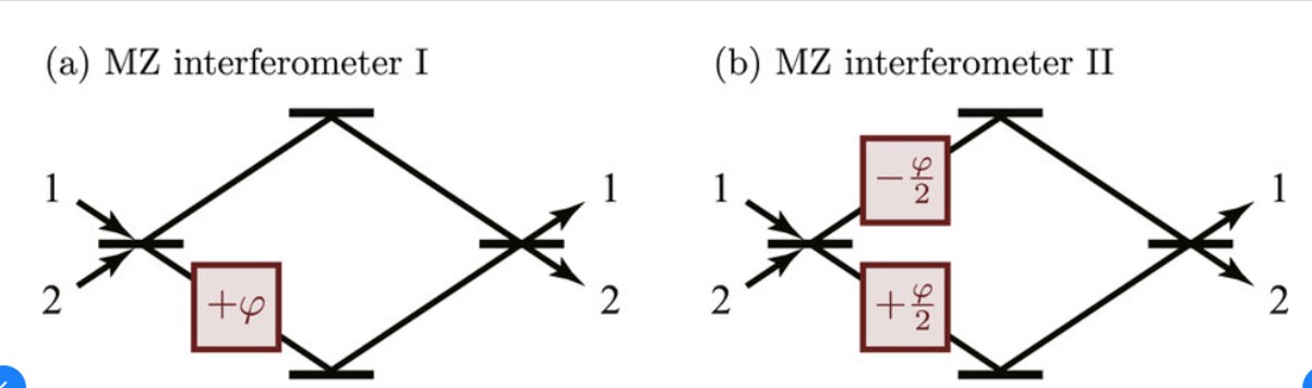
In our experiment, the MZM splits the optical signal and applies a +φ/2 phase shift to one arm and a -φ/2 phase shift to the other. By controlling the relative phase between the two optical waves, constructive or destructive interference occurs when the signals are recombined. This interference determines the resulting optical intensity, which can be detected by a photodiode and interpreted as an amplitude-modulated signal.
The phase shift is induced through the Pockels electro-optic effect. When a voltage is applied across the electro-optic material, an electric field is generated that causes a distortion of the crystal lattice. This distortion alters the polarization response of the material, resulting in a change in the refractive index. The change in refractive index directly modifies the optical phase accumulated along the modulator arms.
The optical phase accumulated over a waveguide of length ( L ) is given by
\[\varphi = \frac{2\pi n L}{\lambda}\]A change in the refractive index therefore produces a corresponding phase shift
\[\Delta \varphi = \frac{2\pi \Delta n L}{\lambda}\]This relationship shows that electrically induced changes in the refractive index lead to controlled phase modulation, enabling the MZM to convert an electrical signal into an intensity-modulated optical signal.
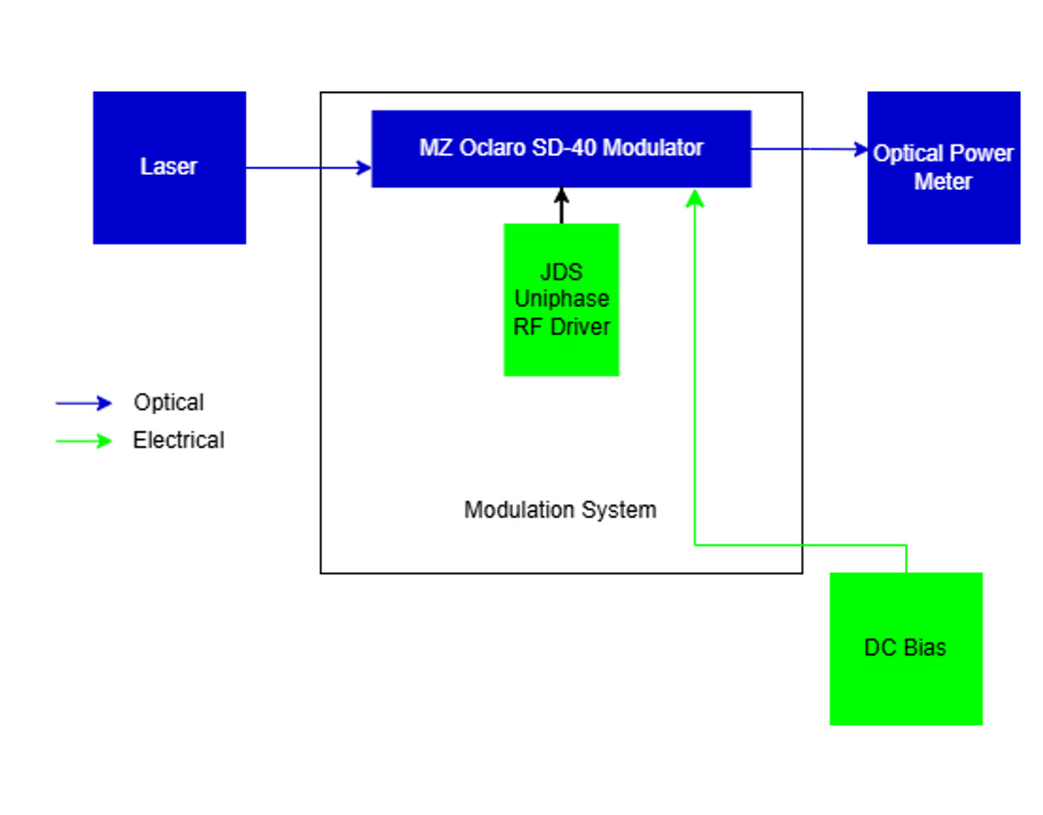
The Mach–Zehnder modulator (MZM) was characterized to establish key device parameters including insertion loss (IL) and half-wave voltage (Vπ). These measurements provided a baseline understanding of modulation efficiency and biasing requirements for high-speed operation.
The test setup plan was as shown below:
The normalized Transfer Function (TF) is shown below:
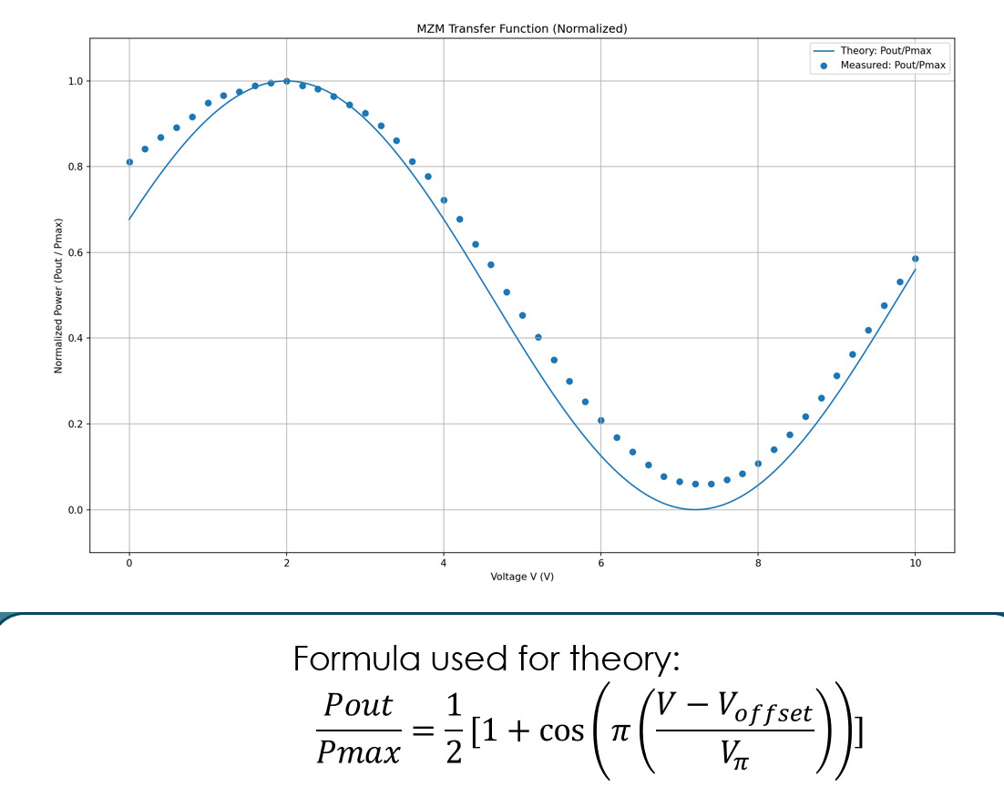
Insertion Loss Calculation
\[IL(\text{dB}) = P_{\text{ref}}(\text{dBm}) - P_{\text{max}}(\text{dBm})\] \[= 9.63 - 2.39\] \[= 7.24\ \text{dB}\]Half-Wave Voltage Calculation
\[V_{\pi} = \left| V_{p,\text{max}} - V_{p,\text{min}} \right|\] \[= \left| 2 - 7.2 \right|\] \[= 5.2\ \text{V}\]Extinction Ratio Calculation
\[P_1 = 2.39\ \text{dBm}\] \[= 10^{2.39/10}\] \[= 1.733\ \text{mW}\] \[P_0 = -9.83\ \text{dBm}\] \[= 10^{-9.83/10}\] \[= 0.104\ \text{mW}\] \[\mathrm{ER(dB)} = 10 \log_{10}\left(\frac{P_1}{P_0}\right)\] \[= 10 \log_{10}\left(\frac{1.733}{0.104}\right)\] \[= 12.22\ \text{dB}\]Phase 2 — BPG Electrical Eye Diagram
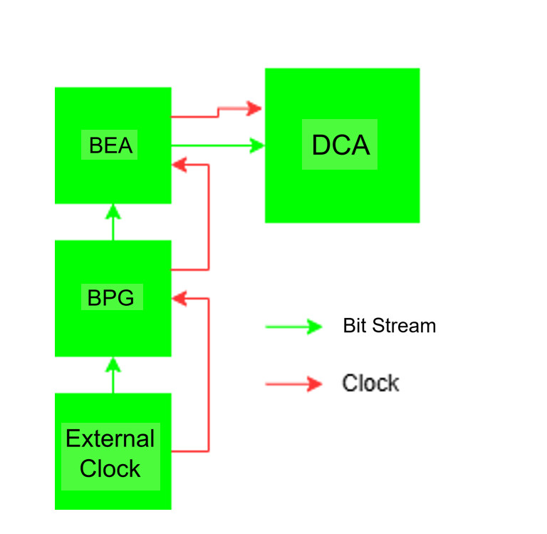
A Bit Pattern Generator (BPG), synchronized to an external clock, was connected to a Bit Error Analyzer (BEA), which interfaced with a Digital Communication Analyzer (DCA) to capture electrical eye diagrams and evaluate the signal-to-noise ratio (SNR) at data rates up to 70 Gbps.
The test set up is shown below:
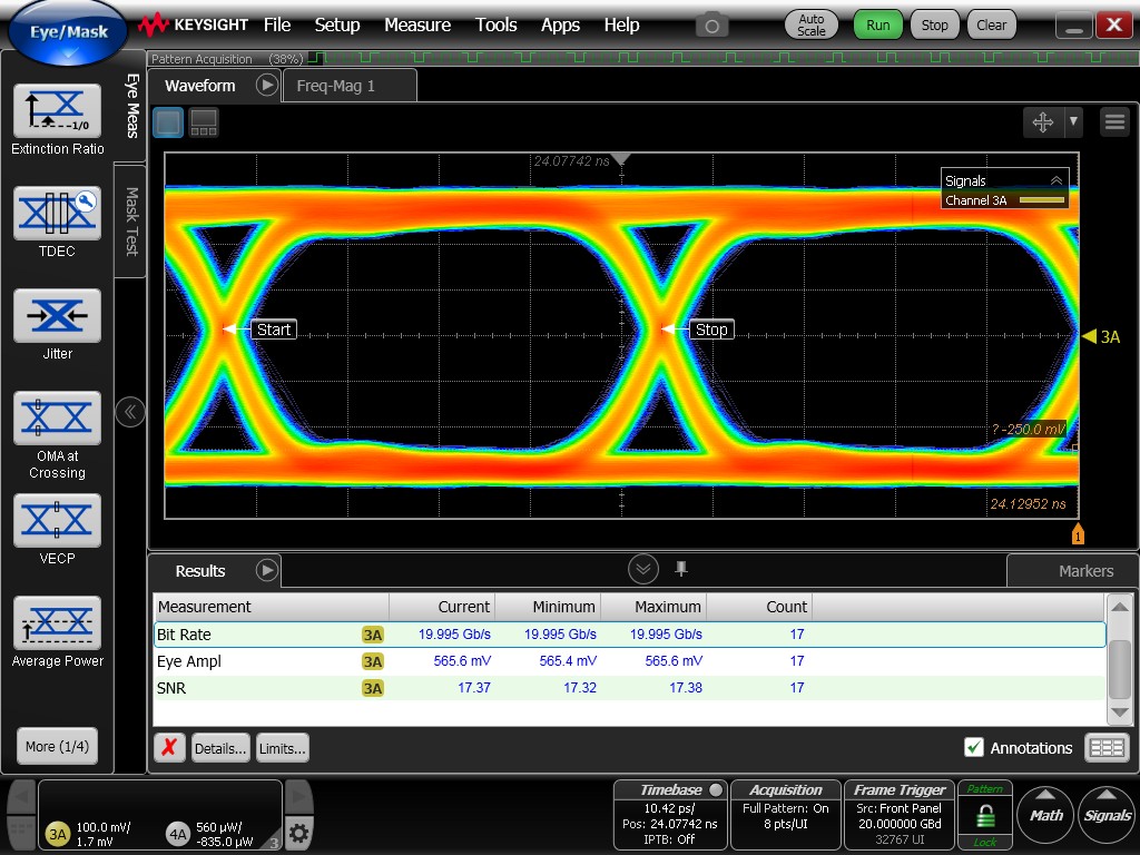
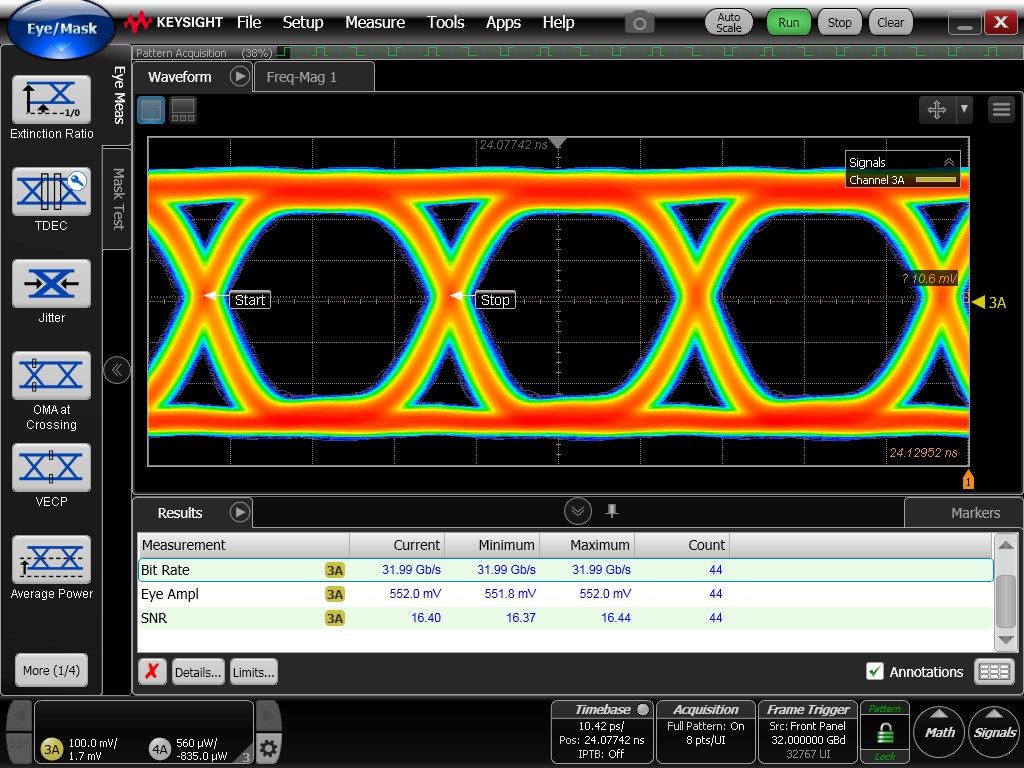
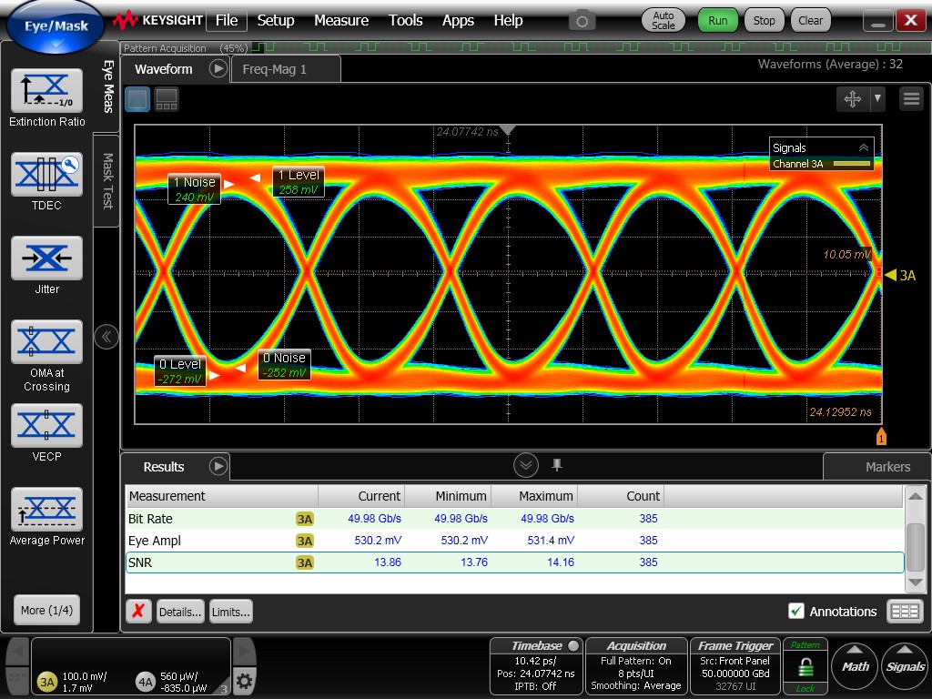
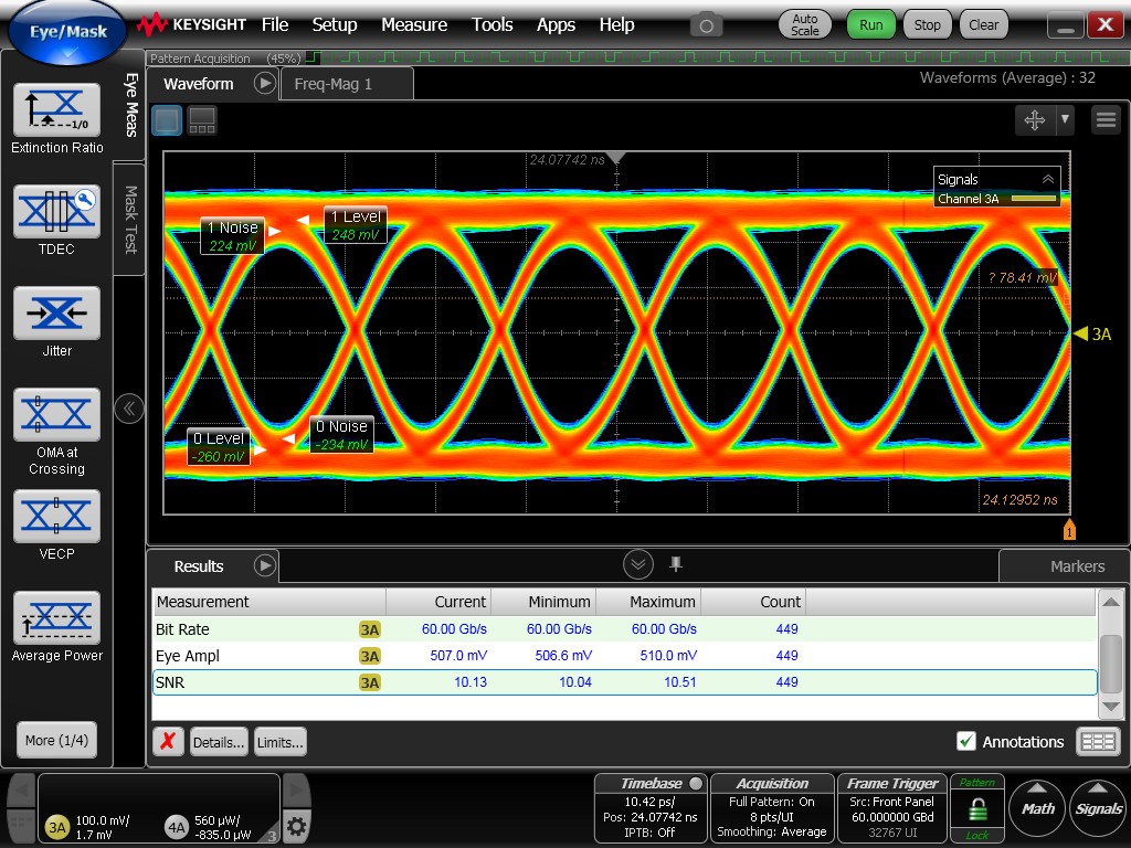
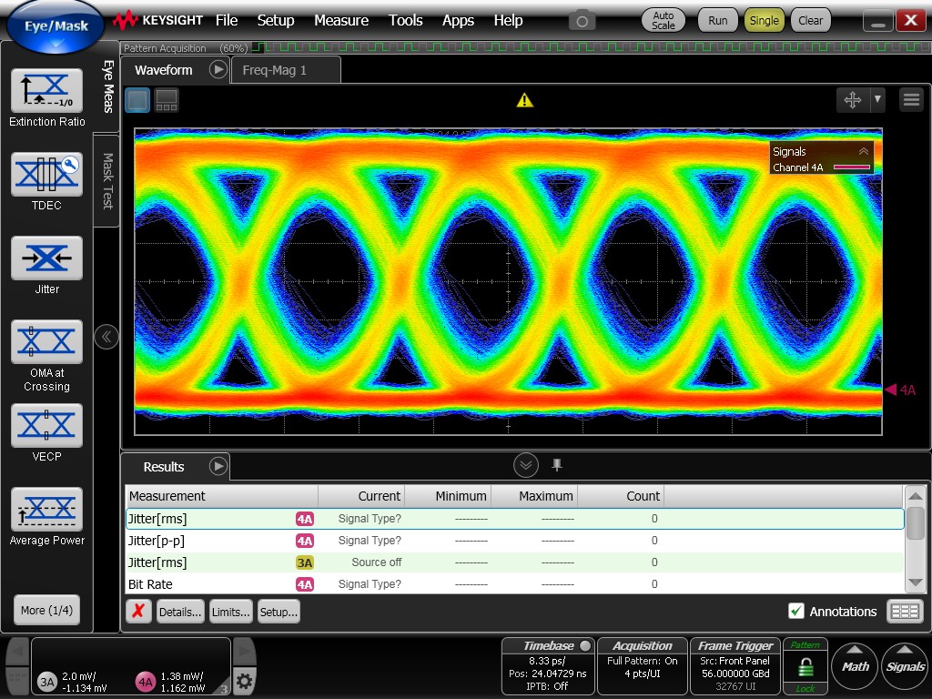
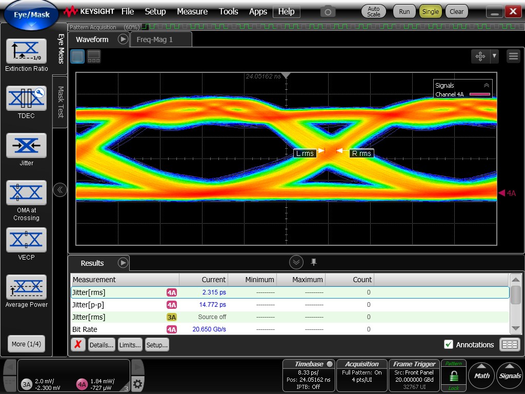
The resulting electrical eye diagrams for data rates of 20, 32, 50, 60, and 70 Gbps are shown below. Since On-Off Keying (OOK) is employed, the baud rate is equal to the bit rate. In contrast, for PAM-4 modulation, the bit rate would be twice the baud rate.
20Gbps SNR 17.37
32Gbps SNR 16.40
50Gbps SNR 13.86
60Gbps SNR 10.13
70Gbps SNR 7.23
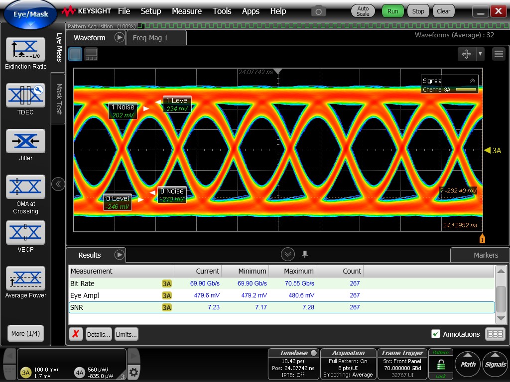
The SNR decreases with increasing data rate as higher bandwidth is required to preserve fast signal transitions, increasing susceptibility to noise and intersymbol interference (ISI).
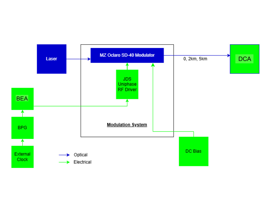
Phase 3 — IM/DD MZM
For this experiment, an IM/DD MZM setup was evaluated at three data rates over fiber lengths of 0 km, 2km, and 5 km.
The test setup is shown below:
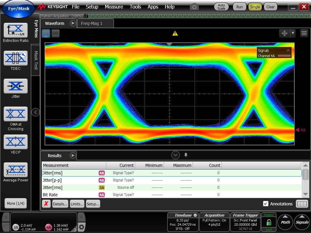
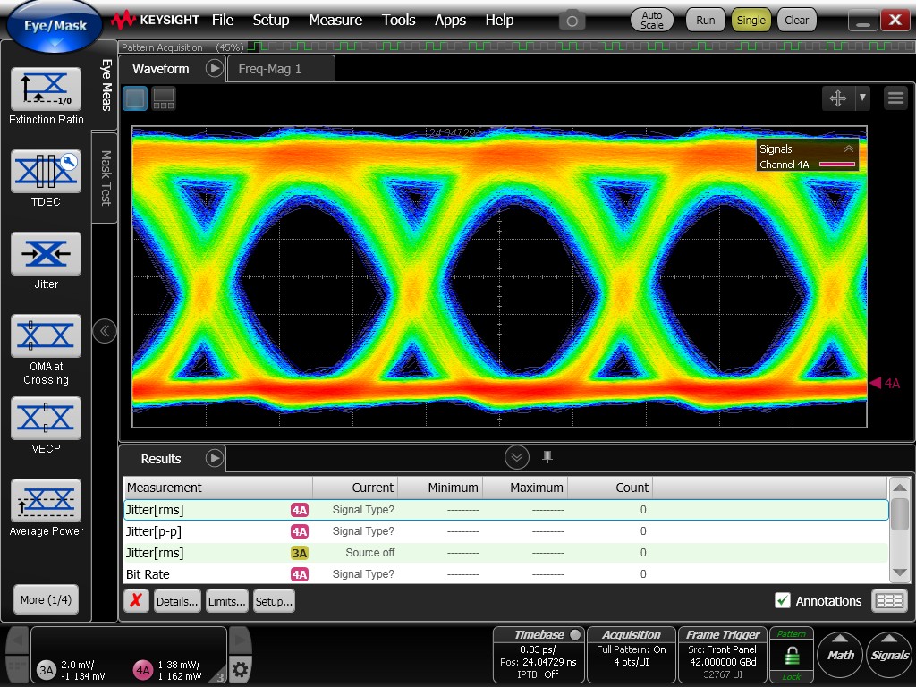
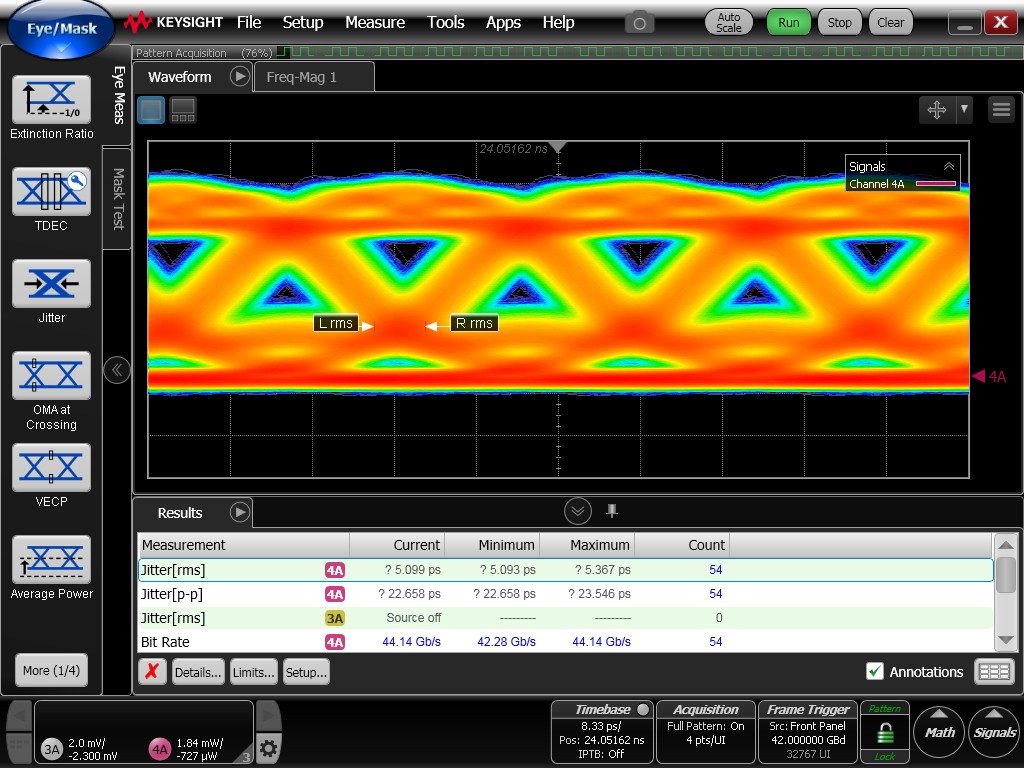
The resulting optical eye diagrams for the 0km fiber optic capbles are shown below for 20, 42, 56 Gbps respectively
0km
20Gbps
42Gbps
56Gbps
Although the eye diagrams remain reasonably open, they exhibit noticeably degraded quality compared to the previously measured electrical eye diagrams. Increased timing jitter is observed, resulting in thicker eye traces and reduced clarity.
5km
20Gbps
42Gbps
56Gbps
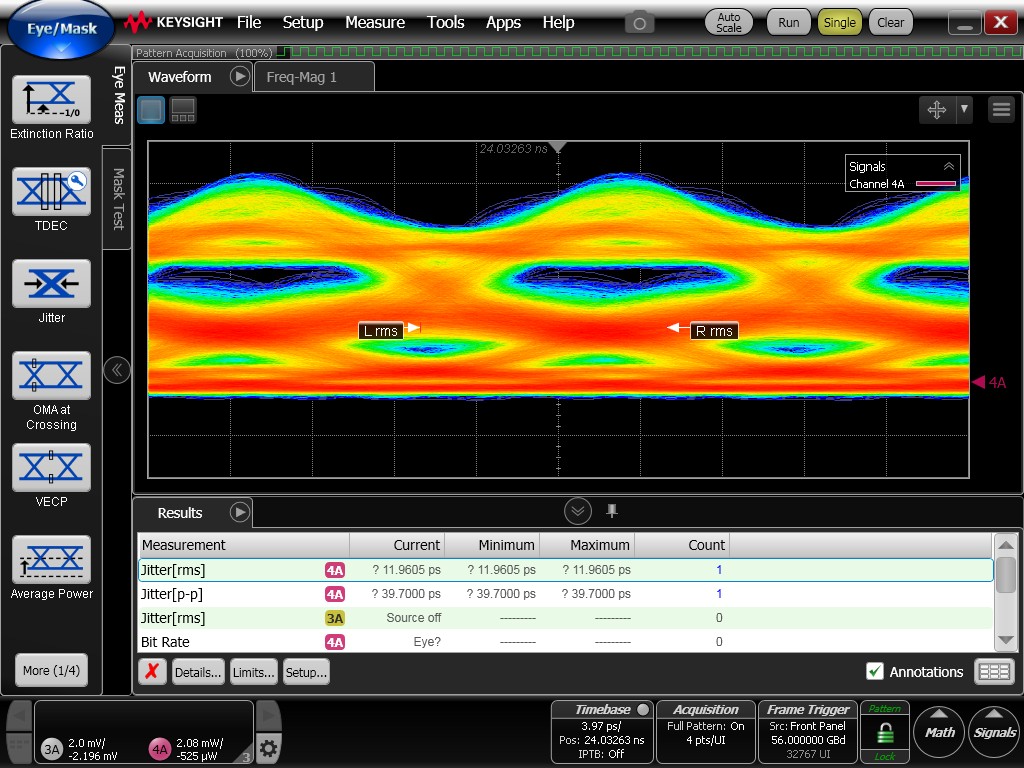
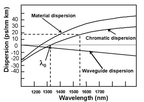
The measured eye diagrams no longer resemble ideal eye openings, which is expected since this experiment was performed in the C-band. At these wavelengths, optical signals are more susceptible to chromatic dispersion over kilometer-scale fiber lengths. For this reason, the O-band is commonly used in industry for IM/DD systems, as it operates near the fiber’s zero-dispersion wavelength. The C-band was used in this experiment due to its near-zero optical attenuation in standard single-mode fiber (SMF).
Chromatic dispersion occurs when different wavelengths within a light signal propagate at slightly different velocities through an optical fiber, causing the signal to spread out in time and become distorted.
In this system, chromatic dispersion arises from two main mechanisms. First, the optical source is not perfectly monochromatic. Although the laser is centered at 1550 nm, small wavelength variations exist around the carrier. Over long fiber lengths, slower wavelength components from earlier symbols can overlap with faster components from later symbols, resulting in ISI.
Second, chromatic dispersion is introduced by amplitude modulation itself. The optical carrier frequency is given by
\[f_0 = \frac{c}{\lambda}\] \[= \frac{3.0 \times 10^8}{1550 \times 10^{-9}}\] \[\approx 193\ \text{THz}\]Let the modulated optical electric field be expressed as
\[E(t) = A_0 \left[ 1 + m \cos(\Omega t) \right] \cos(\omega_0 t)\]Expanding the expression yields
\[E(t) = A_0 \cos(\omega_0 t) + m A_0 \cos(\Omega t)\cos(\omega_0 t)\]Using the identity
\[\cos(a)\cos(b) = \frac{1}{2}\left[\cos(a+b) + \cos(a-b)\right]\]the final form of the electric field becomes
\[E(t) = A_0 \cos(\omega_0 t) + \frac{m A_0}{2}\cos\big((\omega_0+\Omega)t\big) + \frac{m A_0}{2}\cos\big((\omega_0-\Omega)t\big)\]This shows that amplitude modulation generates upper and lower sidebands at different frequencies (and therefore different wavelengths), which propagate at different speeds in the fiber and lead to chromatic dispersion.
One may wonder why the O-band does not significantly suffer from chromatic dispersion. Chromatic dispersion is the combined effect of two mechanisms: material dispersion and waveguide dispersion.
At shorter wavelengths, material dispersion is negative while waveguide dispersion is close to zero. As the wavelength increases, material dispersion increases, whereas waveguide dispersion decreases. In the O-band, these two effects approximately cancel each other, resulting in a chromatic dispersion that is near zero.
As the wavelength continues to increase into the C-band, material dispersion grows more rapidly than waveguide dispersion decreases. Consequently, the cancellation no longer occurs, and the resulting chromatic dispersion becomes non-zero. This behavior is illustrated in the figure below.
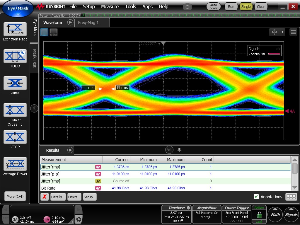
The best performance in terms of both data rate and transmission distance with a clear eye diagram was 42Gbaud over a 2km link. This was achieved in the C-band without DSP.
Phase 4 - TFLN Waveguide Crossing Simulations
In this section, we used Lumerical simulations to evaluate the performance of TFLN waveguide crossings in the O-band under three different temperature conditions. The analysis focused on insertion loss (IL), crosstalk (Xtalk), and reflections. Additionally, electric field intensity heat maps were examined at both the waveguide crossing region and the tapered sections to better understand field distribution and propagation behavior.
Why TFLN and Waveguide Crossings are Important
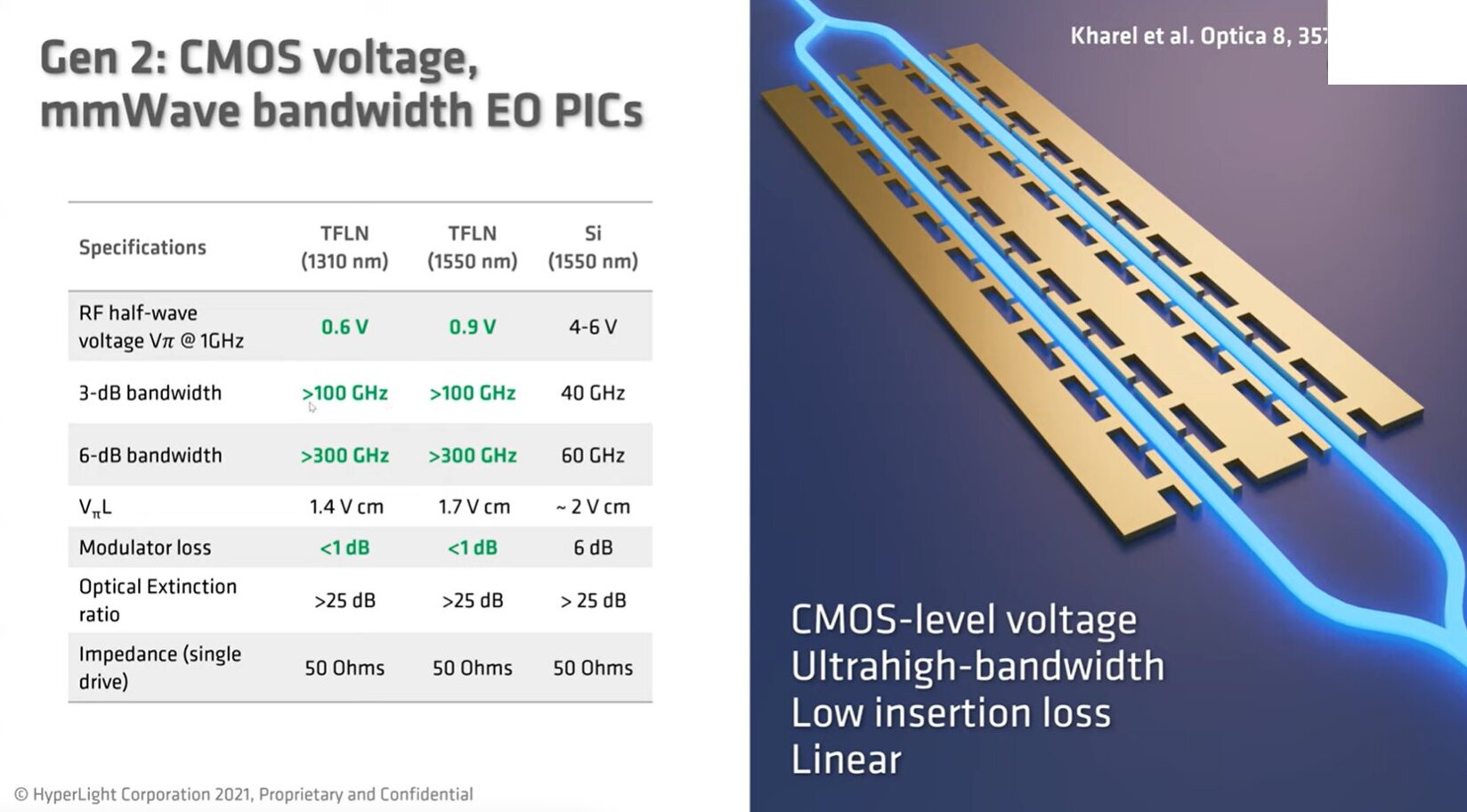
First, it is important to understand why thin-film lithium niobate (TFLN) and waveguide crossings are attractive technologies for modern photonic integrated circuits (PICs). TFLN is a thin-film implementation of lithium niobate, as opposed to traditional bulk lithium niobate used in conventional Mach-Zehnder modulators (MZMs). By reducing the material thickness and increasing optical confinement, TFLN enables more compact and densely integrated photonic chips while improving electro-optic performance.
The phase modulation induced by the electro-optic (Pockels) effect can be expressed as:
\[\Delta \varphi = \frac{2\pi}{\lambda} \Delta nL\]where $\lambda$ is the optical wavelength, $L$ is the interaction length, and $\Delta n$ is the refractive index change caused by the applied electric field. The refractive index change is proportional to the electro-optic coefficient $r_{33}$ and the RF electric field $E_{RF}$
\[\Delta n \propto r_{33} \cdot E_{RF}\]The electric field between electrodes is approximately:
\[E_{RF} = \frac{V}{d}\]where $V$ is the applied voltage and $d$ is the electrode separation. Because TFLN allows electrodes to be placed closer to the optical mode, the electric field experienced by the light increases for the same applied voltage. This enables the same phase shift to be achieved with a lower voltage, reducing the required half-wave voltage ($V_\pi$) and improving power efficiency.
Another important advantage of TFLN is increased modulation bandwidth. The electrode structure behaves electrically like a transmission line with capacitance approximately given by:
\[C \approx \frac{\varepsilon A}{d}\]where $\varepsilon$ is the permittivity, $A$ is the electrode area, and $d$ is the electrode separation. Because stronger electro-optic interaction allows shorter device lengths, the electrode area is reduced, which decreases the effective capacitance. The electrical bandwidth is related to the RC time constant:
\[f_{3dB} = \frac{1}{2\pi RC}\]Reducing the capacitance increases the 3-dB bandwidth, enabling higher-speed modulation and supporting larger baud rates. Additionally, shorter device lengths reduce RF propagation distance, which minimizes microwave loss and improves high-frequency performance.
As photonic devices become smaller and more densely integrated using TFLN technology, waveguide crossings become increasingly important. Dense optical routing requires careful analysis of insertion loss (IL), crosstalk (Xtalk), and reflections to ensure signal integrity is maintained in complex integrated photonic circuits.
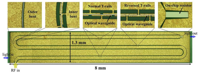
For reference, the figure below shows a TFLN structure.
Before discussing waveguide crossings in greater detail, let’s dive into Why TFLN is used over Silicon Photonics, and why TFLN is called the silicon of photonics.
Silicon dominates the electronic field, but why is it not the answer in the photonics world? According to HyperLight Corp, there are three axes to scale data rate: spectral efficiency, number of channels, and symbol rate.
The following is shown in the picture below from HyperLight’s YouTube channel.
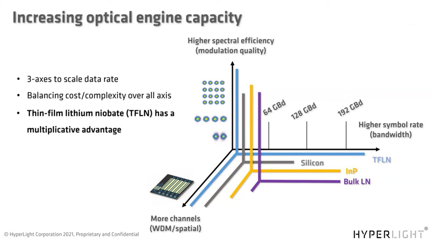
Increasing one or more of these axes increases the total optical engine capacity. Bulk LN experiences drawbacks in the number-of-channels axis due to its large device size, but performs well in the spectral efficiency and symbol rate axes. TFLN performs the best across all three axes. Silicon, however, performs strongly in the number-of-channels axis due to compact integration, but lacks performance in symbol rate (bandwidth) and in spectral efficiency (modulation quality). The reasons are discussed below.
First, let’s look at the bandwidth limitation. Unlike TFLN or LN, silicon modulators rely on the free-carrier plasma dispersion effect. This means modulation is achieved by changing the carrier concentration inside a PN junction. In carrier-injection devices, the carriers have a finite recombination lifetime $\tau$, typically on the order of nanoseconds. The small-signal 3 dB bandwidth can be approximated as:
\[f_{3dB} = \frac{1}{2\pi \tau}\]For example, if $\tau = 1 \text{ ns}$,
\[f_{3dB} \approx \frac{1}{2\pi (1 \times 10^{-9})} \approx 160 \text{ MHz}\]Even if $\tau = 0.1 \text{ ns}$,
\[f_{3dB} \approx 1.6 \text{ GHz}\]This shows why carrier-injection devices are not suitable for very high symbol rate operation.
Secondly, the lower modulation efficiency means a higher voltage $V_{\pi}$ is typically required to achieve the same phase shift. TFLN and LN use the Pockels effect, which allows efficient phase modulation without changing carrier density. Silicon does not naturally exhibit a strong Pockels effect. Instead, its refractive index is related to the material permittivity:
\[n = \sqrt{\varepsilon}\]where
\[\varepsilon = \varepsilon' + j\varepsilon''\]The imaginary component $\varepsilon’’$ introduces absorption loss (free-carrier absorption). This means that increasing the phase shift also increases optical loss. As a result, more drive voltage is required and modulation linearity is reduced compared to TFLN.
This comparison is summarized in the picture below from HyperLight’s YouTube channel.
For more information on HyperLight, I have attached their website below.
Lets get back to Waveguide Crossings
Waveguide crossings enable dense optical routing by allowing multiple light paths to intersect within a photonic integrated circuit, similar to vias or wire crossings in electronic integrated circuits. Rather than directly increasing transmission speed or bandwidth, waveguide crossings improve scalability by allowing more signals and components to fit on the same chip without significantly degrading performance. In other words, they make it possible to build a more densely integrated photonic chip while keeping losses and signal distortion low enough for the system to operate efficiently.
However, crossings introduce potential performance tradeoffs such as insertion loss (IL), crosstalk (Xtalk), and reflections, which must be carefully analyzed to maintain signal integrity. In TFLN photonic platforms, waveguide crossings are fabricated from the same thin-film lithium niobate waveguide structures used throughout the photonic circuit, including modulators and routing components.
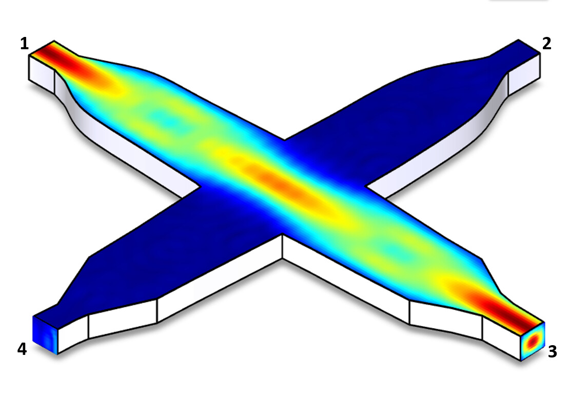
The figure below provides a clear visual representation of a waveguide crossing. Stream A is from port 1 to port 3 and stream B is from port 2 to port 4.
We then used Lumerical to simulate IL, Xtalk and reflection through the O-Band at 27, 55, and 86 degrees celcius.
This figure shows the simulated insertion loss (IL) of a TFLN waveguide crossing across the O-band wavelength range under different thermal conditions (27°C, 55°C, and 85°C). Insertion loss represents the optical power reduction between the input and output ports, primarily caused by scattering, reflections, and crosstalk introduced by the crossing geometry.
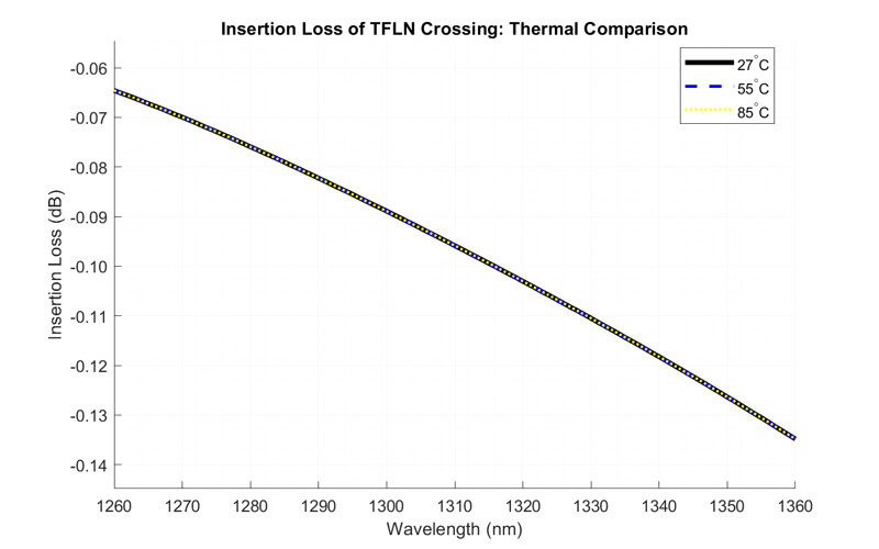
Results show that insertion loss remains below approximately 0.14 dB across the wavelength range, indicating an efficient crossing design with minimal power penalty. The loss becomes slightly more negative as wavelength increases, which can be attributed to the expansion of the optical mode field diameter at longer wavelengths. As the mode expands, the optical beam interacts more strongly with the crossing region, leading to increased scattering and therefore higher loss.
The nearly overlapping curves for different temperatures demonstrate that the crossing is relatively insensitive to thermal variations, suggesting robust performance for practical integrated photonic applications.
Xtalk represents optical power that unintentionally couples into the wrong output path when light passes through a waveguide crossing. Ideally, all optical power should remain in the intended transmission path; however, due to mode overlap and scattering at the crossing region, a small portion of the optical field can leak into perpendicular waveguides.
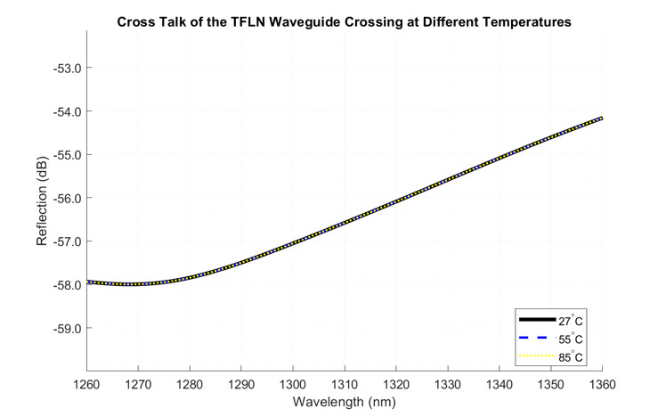
The results show that crosstalk remains well below -40 dB across the entire wavelength range, reaching approximately -57 dB at the target wavelength. This indicates very low unwanted coupling and demonstrates that the crossing design maintains strong signal isolation.
A slight increase in crosstalk is observed at longer wavelengths. As wavelength increases, the optical mode expands spatially, increasing overlap between intersecting waveguides and allowing more energy to leak into unintended ports. The nearly identical curves across different temperatures suggest that the design is relatively insensitive to thermal variations.
Reflection represents the portion of the optical signal that is reflected backward toward the input port when light encounters discontinuities within the waveguide crossing. In practical terms, this corresponds to optical power that travels back toward the transmitter or receiver instead of continuing forward. Excessive reflection can interfere with subsequent data symbols by introducing delayed optical energy that overlaps with future time slots, potentially degrading signal integrity.
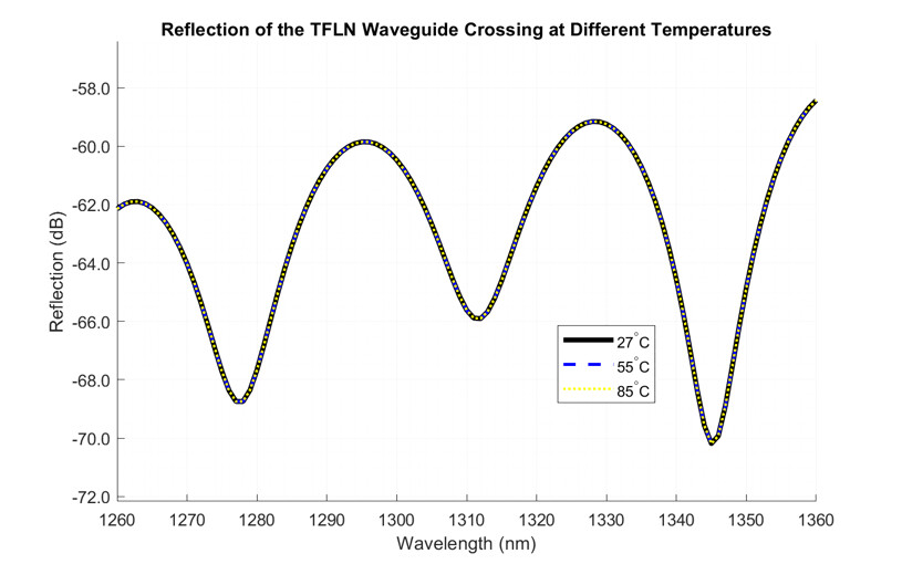
The results show reflection levels around approximately -66 dB at the target wavelength, indicating very low back-reflected power and good impedance matching within the structure. An oscillatory behavior is observed across the wavelength range, which is attributed to wavelength-dependent phase changes leading to alternating constructive and destructive interference within the crossing geometry. The nearly identical curves across different temperatures suggest that reflection performance is relatively insensitive to thermal variations.
To better understand the optical behavior within the TFLN waveguide crossing, electric field intensity distributions were simulated to visualize how the optical mode propagates and interacts with the device geometry. These heat maps provide insight into mode confinement and how structural features influence optical performance. The left image shows the electric field intensity at the waveguide cross-section, while the right image shows the field distribution at the tapered end of the structure.
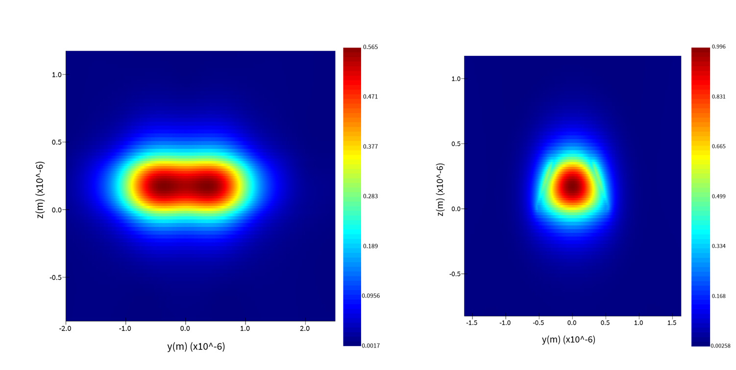
The cross-section field distribution (left) shows a relatively extended optical mode profile, where the optical energy spreads laterally within the waveguide. This represents the baseline propagation condition before strong geometric shaping occurs. A wider mode profile increases interaction with surrounding structures, which can contribute to scattering or coupling effects if not properly managed.
At the tapered end (right), the optical mode becomes more tightly confined due to the trapezoidal taper geometry with approximately a 70-degree sidewall slope. This gradual geometric transition compresses the optical field and increases peak intensity while avoiding abrupt discontinuities. The taper effectively performs a spatial mode transformation, helping maintain efficient coupling and minimizing reflections or additional loss. This controlled confinement contributes to improved signal integrity and supports scalable dense photonic integration.
Next Phase - Upcoming work: TFLN Waveguide Crossing Chip & Full IM/DD TX System
The next phase of the project is to experimentally characterize TFLN modulators and waveguide crossings on chips in order to evaluate their performance, benefits, and limitations. These measurements will be directly compared with results obtained from Lumerical simulations to assess model accuracy and identify discrepancies. The final stage of the project will consist of implementing a complete IM/DD system incorporating TFLN modulation and waveguide crossings.